A CMOS-based chip that integrates silicon quantum dots and multiplexed readout electronics

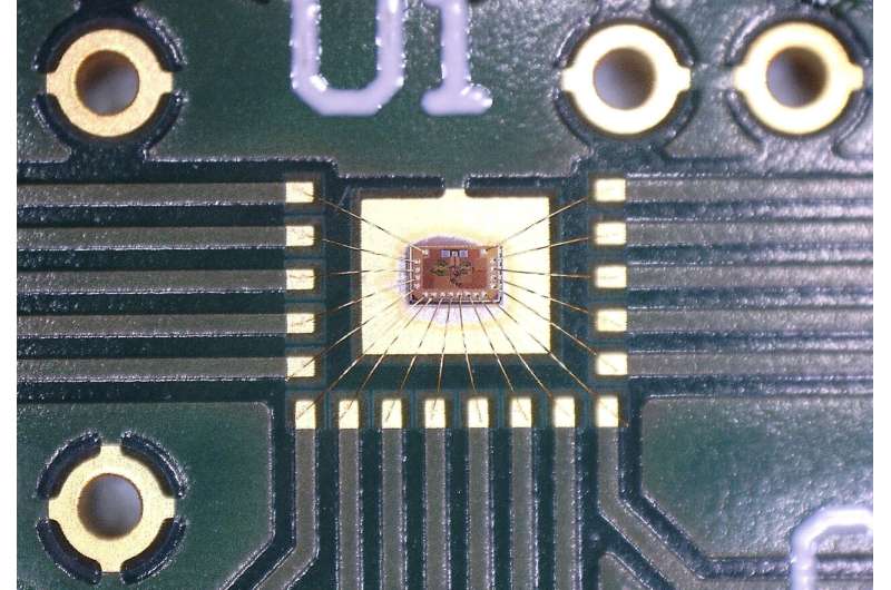
Researchers at École Polytechnique Fédérale de Lausanne (EPFL) and the Hitachi Cambridge Laboratory have recently designed an integrated circuit (IC) that integrates silicon quantum dots with conventional readout electronics. This chip, introduced in a paper published in Nature Electronics, is based on a 40-nm cryogenic complementary metal-oxide semiconductor (CMOS) technology that is readily and commercially available.
“Our recent paper builds on the expertise of the two groups involved,” Andrea Ruffino, one of the researchers at EPFL who carried out the study, told TechXplore. “The goal of our group was to build cryogenic (Bi)CMOS integrated circuits for readout and control of quantum computers, to be co-packaged or co-integrated in the final stage with silicon quantum processors. On the other hand, the team at the Hitachi Cambridge Laboratory have been studying silicon quantum devices for many years.”
Ruffino and his colleagues at EPFL joined forces with the team at the Hitachi Cambridge Laboratory with the common goal of uniting classical circuits and quantum devices on a single chip. Their paper builds on some of their previous efforts, including the proposal of cryogenic CMOS ICs for quantum computing, as well as the realization of fast-sensing and time-multiplexed sensing of silicon quantum devices.
“In our new paper, we tried to propose a fully-integrated circuit version with the goal to demonstrate a scalable architecture for quantum device readout, the co-integration of classical electronics and quantum devices in a single chip in an industrial technology, integrated gate-based dispersive readout at microwave frequencies and finally time-, frequency- and combined time-/frequency-multiplexed readout,” Ruffino explained.
The primary objective of the recent study by Ruffino and his colleagues was to combine the fast-sensing and time-multiplexing techniques devised by the team at the Hitachi Lab, to achieve two-dimensional (i.e., time and frequency) multiplexed sensing. To achieve this, they built a 2D transistor array and applied both these techniques to it.
“We also wanted to integrate all the components introduced in our previous works (i.e., sensors, control/access mechanisms and devices) into one single chip, using standard manufacturing technology,” Tsung-Yeh Yang, a researcher at the Hitachi Cambridge Laboratory involved in the study, told TechXplore. “Hence, the prototype we demonstrated can be readily scaled up.”
The chip designed by the researchers is made of CMOS transistors that resemble those used to fabricate smartphones and other common electronic devices. In contrast with conventional transistors, however, the ones integrated inside the new chip operate at cryogenic temperatures (i.e., at 50 mK) and also contain an array of silicon quantum dots.
“By sending a microwave signal to the gate of the quantum devices and reading the reflected signal response, the state of the quantum devices can be detected,” Ruffino explained. “In this chip, the array of nine quantum devices is divided in three rows and three columns. Each row is connected to a microwave resonator responsive at a different frequency, giving a frequency-multiplexing feature, and each column is connected to access transistors that allow to connect/disconnect the quantum devices, thus giving a time-multiplexing feature.”
The unique design employed by Ruffino and his colleagues allows their chip to simultaneously read multiple quantum devices connected by a single wire and at different frequencies. In addition, the devices to be read out can be individually selected through the access transistors.
“The chip contains two main modules: a device module and a sensor module,” Yang said.
“The device module is built with a 40nm bulk silicon metal–oxide–semiconductor field-effect transistor (MOSFET) 2D array, while the sensor module is built with metal inductor-capacitor (LC) resonator as the electrometer.”
Remarkably, the researchers’ chip integrates all the elements necessary to read-out information, including quantum devices, classical transistors and microwave resonators. In contrast with other previously developed chips, the IC can be used to readout larger quantum systems, while retaining a flexible architecture.
“The structure of our chip is based on the dynamic random-access memory (DRAM) architecture, i.e., a row-column structure, to control/access the MOSFET array,” Yang said.
“The first advantage of using DRAM architecture is that the number of control lines only scales sublinearly with the number of FETs, instead of scaling linearly for one-line-one-FET case. The second is that electrical states of the FETs are sensed by the LC resonators using microwave frequency reflectometry technique, which is faster, with higher resolution and fewer footprint on the chip compared to conventional d.c. transport measurement.”
A key advantage of the new chip is that its two modules (i.e., the device and sensing modules) are combined using standard and commercially available 40nm CMOS technology. This means that in the future it could easily be manufactured on a large-scale.
“The 40-nm bulk silicon MOSFETs we used behave like typical FETs at room temperature,” Yang said. “However, we found that quantum dots (QDs), which is the foundation of building silicon-based quantum bits (qubits), can be induced at deep cryogenic temperatures (
Using their IC, the researchers were able to demonstrate 2D time and frequency multiplexed sensing. These results demonstrate that 2D arrays of silicon-based quantum dots can be fabricated, controlled, and monitored using existing electronic components, such as in CMOS technology.
“I think the most important achievements of this work are the demonstrations that all the elements required for readout (i.e., quantum devices, classical transistors, microwave resonators, etc.) can be integrated on a single integrated circuit in commercial technology operating at 50 mK, that gate-based microwave dispersive readout is possible in a single integrated chip, and that the proposed architecture with combined time- and frequency-multiplexing allows to readout greater numbers of quantum devices while minimizing the number of required wires,” Ruffino said.
In the future, the unique architecture introduced by this team of researchers could be used to read out large 2D arrays of silicon quantum dots, as well as qubits. Ultimately, it could thus help to address some of the scaling-related limitations of existing silicon quantum processors.
In their next studies, Ruffino, Yang and their colleagues plan to explore the possibility of integrating high-fidelity silicon-based qubits into their proposed chip architecture. Their hope is to demonstrate control/access and readout of a two-dimensional qubit array using a DRAM architecture, which can be manufactured using existing electronic components.
“Our plans for future development in this area mainly lie in the extension of this work to larger arrays and in the improvement of several characteristics of our demonstration, such as the quality of the quantum devices and the quality factor of microwave resonators,” Ruffino said. “Moreover, our final research goal will be to demonstrate our architecture on a system implementing co-integrated silicon qubits.”
Conclusion: So above is the A CMOS-based chip that integrates silicon quantum dots and multiplexed readout electronics article. Hopefully with this article you can help you in life, always follow and read our good articles on the website: Ngoinhanho101.com


